
文獻(xiàn)標(biāo)識(shí)碼: A
文章編號(hào): 0258-7998(2013)09-0061-02
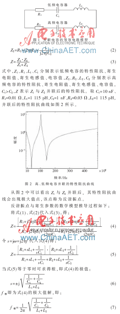
隨著印制電路板(PCB)集成度的提高,寄生參數(shù)會(huì)破壞PCB電源分配網(wǎng)絡(luò)(PDN)的穩(wěn)定性[1],PDN的阻抗ZPDN會(huì)產(chǎn)生尖峰(反諧振點(diǎn)),參考文獻(xiàn)[2]通過去耦電容削弱ZPDN的尖峰并將其推移至PCB的非工作頻段,指出了并聯(lián)去耦電容的等效特性阻抗會(huì)產(chǎn)生反諧振點(diǎn),且該點(diǎn)不可以大于目標(biāo)阻抗。參考文獻(xiàn)[3]總結(jié)了各種電容器隨著頻率升高,其特性阻抗、有效容值受寄生電阻的影響;參考文獻(xiàn)[4]是從場(chǎng)角度研究電容特性阻抗與寄生參數(shù)的關(guān)系,參考文獻(xiàn)[5]采用運(yùn)算放大器來增加電容的有效容值。以上文獻(xiàn)都均未給出寄生參數(shù)和去耦電容特性阻抗反諧振點(diǎn)關(guān)系的完整模型。
參考文獻(xiàn)[6]詳細(xì)描述了單個(gè)電容寄生參數(shù)與特性阻抗之間的關(guān)系;參考文獻(xiàn)[7-8]從等效電路角度計(jì)算出了ZPDN尖峰的頻率位置;參考文獻(xiàn)[9]將PDN等效為微波網(wǎng)絡(luò)計(jì)算出了ZPDN尖峰的頻率位置;上述文獻(xiàn)中,僅給出了寄生參數(shù)變化對(duì)反諧振點(diǎn)的影響的仿真圖形,并沒有給出相應(yīng)數(shù)學(xué)模型。
本文主要在參考文獻(xiàn)[6,8]的基礎(chǔ)上,推導(dǎo)并驗(yàn)證了并聯(lián)電容特性阻抗反諧振點(diǎn)與電容寄生參數(shù)的數(shù)學(xué)模型,即合理選取最佳去耦電容來盡可能壓低反諧振點(diǎn)的阻抗,然后在Cadence開發(fā)環(huán)境中實(shí)施了該方法,從而在選取去耦電容器這一環(huán)節(jié)上給出了重要的理論參考。
1 電容特性阻抗分析
圖1為并聯(lián)電容的等效電路模型[7],阻抗為:
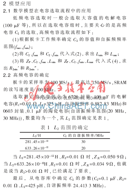
本文從并聯(lián)電容的等效電路模型出發(fā),推導(dǎo)出電容參數(shù)與反諧振點(diǎn)頻率、反諧振點(diǎn)幅度的數(shù)學(xué)模型,然后將此模型應(yīng)用到基于目標(biāo)阻抗的設(shè)計(jì)中。通過簡(jiǎn)單計(jì)算,驗(yàn)證了電容組選取的合理性。此方法簡(jiǎn)單直觀,為高速電路設(shè)計(jì)人員在選擇去耦電容時(shí)提供了有價(jià)值的參考。
參考文獻(xiàn)
[1] POPOVICH M,F(xiàn)RIEDMAN E G,SOTMAN M,et al.On chip power distribution grids with multiple supply voltages for high-performance integrated circuits[J].IEEE Transactions on Very Large Scale Integration(VLSI) Systems,2008,7(16):908-921.
[2] SMITH L D,ANDERSON R E,F(xiàn)OREHAND D W,et al. Power distribution system design methodology and capacitor selection for modern CMOS technology[J].IEEE Transactions on Adcanced Packaging,1999,3(22):284-291.
[3] CHARANIA T,OPAL A,SACHDEV M.Analysis and design of on-chip decoupling capacitors[J].IEEE Transactions on Very Large Scale Integration(VLSI) Systems,2012:1-11.
[4] JIAO D,KIM J H,He Jianqi.Efficient full-wave characterization of discrete high-density multiterminal decoupling capacitors for high-speed digital systems[J].IEEE Transactions on Adcanced Packaging,2008,31(1):154-162.
[5] Gu Jie,HARJANI R,KIM C H.Design and implementation of active decoupling capacitor circuits for power supply regulation in digital ICS[J].IEEE Transactions on Very Large Scale Integration(VLSI) Systems,2009,17(2):292-301.
[6] NOVAK I,NOUJEIM L M,CYR V S,et al.Distributed matched bypassing for board-level power distribution
networks[J].IEEE Transactions on Adcanced Packaging,2002,2(25):230-243.
[7] POPOVICH M,F(xiàn)RIEDMAN E G.Decoupling capacitors for multi-voltage power distribution systems[J].IEEE Transactions on Very Large Scale Integration(VLSI) Systems,2006,14(3):217-228.
[8] KIM J,SHRIGARPURE K,F(xiàn)an Jun,et al.Equivalent circuit model for power bus design in multi-layer PCBs with via arrays[J].IEEE Microwave and Wireless Components Letters,2011,21(2):62-64.
[9] Zhang Yaojiang,OO Z Z,Wei Xingchang,et al.Systematic microwave network analysis for multilayer printed circuit boards with vias and decoupling capacitors[J].IEEE Transactions on Electromagnetic Compatibility,2010,52(2):401-409.